Treatment LCD monitor

Treatment LCD Monitor. At this time computer use familiar and already widely used either for work or entertainment. And of course when talking about computers it will not be far away with a device called a monitor. And today use CRT monitors have started to decrease with the LCD Monitor that despite having a price that is quite expensive but have many advantages than conventional CRT monitors.


Here are a few advantages of LCD monitor is a stylish design, flat screen and a brighter color than convex or crt monitor screen, while also LCD Monitors have many advantages among which have a high resolution so that it can help many people especially those working Visual design field.

There are some special treatment for LCD monitors in this case is for the treatment of LCD monitors, the following are some steps steps:

Use the LCD as needed, Do not use if you do not need so-necessary and do not use it 24 hours nonstop jedanya have no time for any electronic item there during his lifetime (Lifetime). Turn off your LCD monitor when your computer dies, in order to save electricity and also keeps your LCD monitor remain durable.
Use the type that has a grounding electrical power, because it can minimize the damage in the event of lightning strikes. This option is optional.
Perform regular cleaning, at least 2 weeks 1 times, for LCD monitors are always in a state clear of dust and other debris. Remember! to clean it must use a very soft cloth that has spread with a special liquid cleaners LCD monitor. If necessary you can buy special equipment to clean the LCD monitor.
Do not engage in cleanup activities in the state of electricity is still flowing, unplug all cables available on the LCD to avoid things that are not desired. The existence of water coming into the series of LCD monitors will be able to cause fatal damage.
Keep the LCD of the things that contain water such as rain water, drinking water etc.. Because all electronic goods electrical short circuit will occur if water enters into the electronic components.
Keep the LCD of goods containing such magnetic sound system, Persani, HP etc. signals. Because it will be fatal is going to happen Noise or damage which may destroy the layout on the monitor screen.
LCD Save a strategic place and safe from the reach of small children, so that you can not avoid tersenggol LCD or a small toy.
Unplug all cables associated with the computer (including LCD) in the event of rain accompanied by lightning, because lightning can be grabbed via the antenna propagate through the cable TV and electricity.
To protect the screen / LCD screen can use the Screen Protector function prevents dust entry into the LCD and also take care of all sorts of scrapes. Remember to choose the screen protector is not a trace when reopened.
If there is damage to your LCD monitors, LCD submit to the experts. Do not disassemble itself without accompanied by experts in the field of electronics. Module Components including LCD monitors that can be easily damaged. LCD Monitor Service you to the service center to ensure the improvement is good and right.
Good article on the LCD monitor is beneficial treatment.

3 Band Tone Control with LF351

3 Band Tone Control circuit uses an op-amp as an amplifier end. Tone Control circuit is a regulator of tone bass, midrange and treble or 3 band called because it can set the three tones. Filter circuit is applied to the series of "Tone Control 3 band" This type baxandal like the title of this article. 

Results filtering regulator tone or tone control baxandal type is good, because there is no signal level is wasted directly into the ground. Range frequency tones generated from Tone Control 3 band was determined by the configuration of the R and C of the filter section baxandal. As an amplifier on Tone Control The set of three band use traditional IC LF351 has slewrate high and high input impedance. For more details, series 3 Band Tone Control as follows.

Figure Series 3 Band Tone Control

3 band tone control

3 Band Tone Control circuit above using LF351 Op-Amp is used to strengthen the signal after filtering by the filter process baxandal. Level tone Bass, Midrange and Treble settings are determined by potensio R1, R2 and R3. Frequency filter in the circuit above baxandal to 50 Hz bass tone, tone Midrange 1 KHz and 10 KHz for Treble tone.

Video amplifier circuit is simple and can be used. Video amplifier circuit was constructed from 2 pieces of transistors BC550 and BC560. The source voltage used for supplying the video amplifier circuit is 5VDC. Video amplifier circuit is equipped with a powerful regulator which flows through both transistors T1 and T2, the components used to manage these flows are P1 and P2.
Video Amplifier Circuit Diagram
Video Amplifier Circuit Diagrams

Then the video amplifier circuit is also equipped with limiting the maximum current that passes through T1 and T2. The components in black block functions as limiting the maximum current that is passed by the T1 and T2 for no more than 5mA.

Amplifier circuit here is all based on the ic in the gains. Three IC TA7230P, TA7236P, TA7237AP is intregated circuit (IC) which was applied to the power amplifier. Each IC has a different output, different input voltage, all IC TA7230P, TA7236P, TA7237AP is manufactured by Toshiba.


TA7230P, TA7236P, TA7237AP amplifier schematic

Amplifier circuit here is all based on the ic in the gains. Three IC TA7230P, TA7236P, TA7237AP is intregated circuit (IC) which was applied to the power amplifier. Each IC has a different output, different input voltage, all IC TA7230P, TA7236P, TA7237AP is manufactured by Toshiba.

You can see maximum minimum voltage , power output , and other here
TA7230P, TA7236P, TA7237AP amplifier schematic

Frequency to Voltage Converter

Overview of IC LM2917 as Frequency to Voltage Converter
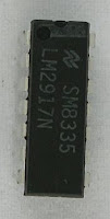
IC LM2917 IC chip is designed specifically as a Frequency to Voltage Converter or Frequency to Voltage converter. In its use to applications Frequency to Voltage Converter IC LM2917 requires few external components.

There are several examples of applications of Frequency to Voltage Converter IC LM2917 is supplied in the LM2917 IC datahseet. In this article series Frequency to Voltage Converter IC also taken from the LM2917 datasheet. The advantages of single chip LM2917 Frequency to Voltage Converter is able to provide instantaneous volt output o at time of frequency change 0 Hz.

Frequency to Voltage ConverterVery easy to apply in measuring the output frequency with the formulation of single-chip Frequency to Voltage Converter VOUT = FIN x VCC x R1 x C1. Then the single-chip LM2917 Frequency to Voltage Converter This configuration requires only the RC only in frequncy doublings. And has an internal zener regulator to aimlessly accuracy and stability in frequency-to-voltage conversion process.

Frequency to Voltage Converter


Feature-owned single-chip LM2917 Frequency to Voltage Converter

  • Reference to ground directly with variable reluctance
  • Op Amp / Comparator with transistor output
  • 50 mA maximum output currents for application directly to the load
  • Frequency doubling untul low ripel
  • Buid in zener
  • Linear output ± 0.3%

Application single chip LM2917 Frequency to Voltage Converter

  • Frequency to Voltage Converter
  • Rotation speed sensor applications
  • Speedometer
  • Tachometer
  • Cruise Control
  • Cluth Control

And other application associated with the measurement of rotation speed or frequency measurements.

Voltage to frequency converter

Voltage to frequency converter
Changing the voltage to frequency scale in the design of an electronic device is sometimes necessary. The series of articles voltage to frequency converter with the XR 4151 is one answer. Voltage to Frequency converter circuit with the XR 4151 is the idea of time in college, when there are projects to create a tool to hatch chicken eggs.


It will be my neighbor also write articles incubators chicken egg-based microcontroller AT89C2051. Maybe there are friends who still remember to this project. Back to the topic of voltage to frequency converter circuit with the XR 4151. IC XR 4151 is a major component of voltage to frequency converter (Voltage to Frequency Converter).
Voltage to frequency converter

From voltage to frequency converter circuit with XR 4151 on the input signal circuit is a DC voltage level. IC XR4151 on voltage to frequency converter circuit serves to convert the voltage level coming into form in the development of the frequency change, where the output frequency range of voltage to frequency converter with the XR 4151 is proportional to the voltage level input voltage to frequency converter circuit with this 4151 XR.

Car Amplifier Care Tips

Car Amplifier Care Tips

car amplifier

Amplifier that work as one of the pillars of car audio does have ipandang performance that can not be underestimated. so we need to know a few things to keep our car amplifiers are not easily damaged. The following tips for creating a durable amplifier.


1. To install an amplifier on the audio systems in vehicles to avoid amplifier from moisture, the way while avoiding the base of potential placement into water vapor. so do not get into the inside of the amplifier resulting in damage to the components inside.

2. There is a good amplifier is used or not stored in a long time alias stored in a warehouse because after all the components within it requires a flow of current in accordance with nature as Conductor supply current to the driver other car audio.

3. Inside the vehicle, an amplifier should also be checked periodically, this is to find out the connection cable attached to the amplifier, amplifier kondiso also working actively to your car audio system.

car amplifier

Entertainment in the form of music, news or even movies, generated from a series of audio devices found in a car. The series device known as a car audio system.
What tool or device contained in car audio system?

  • Car Head Unit - Head unit is the core of a car audio system, part of the car audio system that plays sound. The continued development of technology makes the head unit is no longer only serve as a radio receiver FM / AM CD player and a player, some have additional functions to be able to play MP3s. There is also a car head unit that has the ability to play DVDs complete with monitors and can be connected with IPOD.
  • Power Amplifier - The function of the power amplifier is to amplify the signal coming out of the head unit. In the world of various types of car audio power amplifiers are divided into several classes, such as class A, B, AB, and D. Each class power amplifier has the advantage that its usefulness can be tailored to our needs in building a car audio system. In addition to class division, the division of power amplifiers can also be seen from the number of channels (channels) and the amount of power generated by the power amplifier.
  • Speaker - A device that functions convert electronic signals into audible sound. The speakers were divided into several parts / components, namely, subwoofers, woofers, mid-range, and tweeter. In order for speakers to work properly, required a series of electronic components that serves as a filter (cross over).
  • Processor - With advances in technology processors play a significant role in a car system. Inside there is a processor features like time correction, cross-over-active, etc. equalizer. With the functions it will be very easy at the time of 'tuning' car audioaudio system.

Humidity Sensors with SHT11

Humidity Sensors
Humidity Sensors with SHT11. SHT11 Humidity Sensors is a single chip relative humidity and temperature sensors with multi-sensor module that has been calibrated digital output. Section included a polymer capacity as eleman for relative humidity sensors and a ribbon strain used as temperature sensors.

Output of both sensors are combined and connected on 14-bit ADC and a serial interface on a single chip the same. The sensor output signal aimlessly good with a fast response time. SHT11 Humidity Sensor was calibrated at room denagn humidity accurately using as a reference hygrometer. Calibration coefficients have been programmed into the OTP memory. Coefficient will be used to Calibration output from the sensor during the measurement process.

Humidity Sensors
Humidity Sensors Diagram Block
Sensor system used to measure temperature and humidity are SHT11 Humidity Sensors with 5 Volt voltage source and bidirectonal 2-wire communication. This sensor system has a data path that is used for addressing and reading the command data.

Data collection for each measurement is done by giving orders addressing the microcontroller. Foot serial data that is connected with microcontroller provides a command addressing the pin Data SHT11 Humidity Sensors "00,000,101" to measure relative humidity and "00000011" for temperature measurement. SHT11Humidity Sensor provide humidity and temperature output data on data pins alternately in accordance with the given clock microcontrollers for sensor to work. Sensor SHT11 have ADC (Analog to Digital Converter) in it so that the output data is configured SHT11 Humidity Sensors in the form of digital data and requires no external ADC in data processing on the microcontroller. SHT11 Humidity Sensors data retrieval scheme can be seen in the picture below.

Universal PIC Programmer Circuit
The series of Universal PIC Programmer can be used with software IC-Prog 1:05. Universal PIC programmer circuit is very simple with BC337 transistor 1 fruit, 2 pieces of IC regulators 7805 and 7808 as well as supporting passive components. Universal PIC Programmer series can be supplied with 2 pieces of 9V batteries.

For communication with computer circuit Universal PIC Programmer uses a serial RS232 port of computer. Then for the PIC to be programmed provided 5 lanes for the PIC that is DATA, Clock, Vpp, Vcc and Ground. For more details, can be directly seen in the figure below.

Universal PIC Programmer Circuit diaggram
Universal PIC programmer circuit diagram

The series of Universal PIC Programmer can be used to program the PIC family of 16F84A series, 12C509, 16C765 and the other. Hopefully this series of Universal PIC Programmer can help for friends who want to make PIC programmer.

Solid State Relay Circuit
Solid state relay is a series that functions like a relay hibryd mechanics. Solid state relays is built with insulating an MOC for separate the input and the switch. With Solid state relays we can avoid the occurrence of sparks as it did in the relay can also avoid the occurrence of conventional connection is not perfect because porous contactor as in conventional relays.


The series of solid state relays This is quite simple and we can make in a PCB hole. For more details can be seen in the picture following a series of solid state relays.

Solid State Relay Circuit
Solid State Relay Circuit Diagram

Solid state relay has many advantages including no mechanical friction on the contactor, the connection process only occur when there are crosses zero, there is no spark at the contactor, not noisy, small konsusi flow control, better endurance.

Light Switch Circuit Diagram

circuit diagram
The series of light switches this time slightly different from the voltage of work. The series of light switches can work directly on the AC power network. Light switches are using the main component of TRIAC and LDR. The circuit is very simple and the components were sold in the market.

If you want a light reception sensitivity of this circuit can be arranged then the 3.3 MOhm resistor can be replaced with a variable resistor. For more details can be seen from the following series of images.
Circuit Diagram


With Triac Light Switch series is prisipkerjanya as dimers, but dimers control performed by the reception of light around the LDR. The lower the intensity cayaha received LDR then semkin bright lights. For installation LDR need to be considered so as not exposed to light from the lamp directly.

cheap electronics
Cheap electronics component for amplifier application, it is simple to be made for speaker active . The sound quality even this  Mini Amplifier TDA2030 quite satisfactory for a portable audio system.


"The series of Mini Amplifier TDA 2030 "The series of mini amplifie can reproduce the power output of 14 Watt with 8 Ohm speaker load. The series of mini-amplifier can be supplied with ource voltage of 12 volts - 15 volts DC. more details, see the following series of pictures.

cheap electronics

Daftar komponen
Resistor:

- R1: 150KΩ
- R2: 4.7KΩ
- R3: 100KΩ
- R4: 1Ω 1W
- RA/RB: 100KΩ

Capacitor

- C1: 1µF / 25V
- C2: 2.2µF / 25V
- C3: 100nF
- C4: 22µF / 25V
- C5: 100 µF / 25V
- C6: 220nF
- C7: 2200µF / 35V

IC / Dioda

- IC1: TDA2030 or TDA2030a
- D1/D2: IN4002

Battery Level Monitor Circuit

Battery Level Monitor Circuit

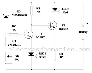
This simple circuit can monitor the charging process in 12 Volt Lead Acid battery or Tubular battery. The status of LED indicates whether the battery is accepting charge or not. It also indicates the full charge condition.


Battery Level Monitor Circuit
Battery Level Monitor Circuit Diagram

The circuit can be incorporated in any battery charger like 6 volt, 9 volt, 12 volt etc. The only change needed is replacement of the Zener ZD with appropriate value. That is for 6 volt charger , use 6.1 volt Zener and for 9 volt charger it should be 9.1 volt Zener.


The circuit is based on the switching of two NPN transistors (BC547) to drive the corresponding LED. Zener diode ZD is connected to the base of T1 so as to switch on T1 when the Zener conducts. This happens only when the battery voltage is above 12 volts. Green LED lights when the battery voltage is normal or battery attains full charge. Resistor R1 and Preset VR adjust the base bias of T1 for smooth switching. When T1 conducts, base of T2 will be pulled to ground and T2 turns off and Red LED extinguishes.

When the circuit is connected to the battery before charging the LED indications will be

1. If the battery voltage is above 12 volts (that is the normal terminal voltage of 13.8), Zener conducts and Green LED lights and Red LED remains off.
2. If the battery voltage is below 12 volts, Zener remains non conducting and Green LED remains off and Red LED lights.
3. When the battery is connected to the charger, and if the battery is accepting charge, Green LED goes off and Red LED remains on. When the battery attains full charge, Green LED lights and Red LED goes off.
4. If the battery is not accepting charge, Green LED never lights, even after the prolonged charging. This indicates that the battery is not attaining the normal terminal voltage above 12 volts.
source [link

Accelerometer Sensor

Accelerometer Sensor
Sensor Accelerometer MMA 3201 is a sensor used to measure the acceleration of motion of the payload when the payload was launched until the payload is delivered to the home again, Sensor Accelerometer MMA 3201 has a resistance to the gravitational force of 20g on the axis X and axis Y.

Sensor Output Accelerometer MMA 3201 is still in the form of analog data so that the need for an ADC to process the data. Data released by Sensor Accelerometer MMA 3201 is a linear form of X and Y axis, the second determines the acceleration motion data payload.

Accelerometer Sensor
Accelerator sensor with MMA 3201

Feature Sensor Accelerometer MMA 3201
  • Sensitivity in two separate axes: 40g X-axis and 40g Y-axis
  • Integral Signal Conditioning
  • Linear Output
  • Ratiometric Performance
  • 4th Order Bessel Filter Preserves Pulse Shape Integrity
  • Calibrated Self-test
  • Low Voltage Detect, Clock Monitor, and EPROM Parity Check status
  • Transducer Hermetically Sealed at Wafer Level for Superior Reliability
  • Robust Design, High Shocks Survivability

AMN12111 - PIR Motion Sensor

AMN12111 - PIR movement sensor
PIR movement sensor module (Passive Infra Red) motion detection sensor AMN12111 is the smallest of objects the size of its shape. PIR motion sensor module (Passive Infra Red) AMN12111 fresneal come equipped with a lens. PIR motion sensor module (Passive Infra Red) AMN12111 has advantages can be directly connected to the microcontroller or other actuator driver.

PIR movement sensor module (Passive Infra Red) AMN12111 has a sensitivity that is very sensitive to changes in motion around it. PIR movement sensor module (Passive Infra Red) AMN12111 very suitable when applied to security systems. The price of the PIR movement sensor module (Passive Infra Red) AMN12111 not quite expensive. readily available in the market. For those of you who want to make a motion detection sensor. PIR movement sensor module (Passive Infra Red) AMN12111 is much easier and more practical than you have to make a series of Infra Red with the Tx and Rx.

Direction Sensor - CMPS03

Direction Sensor - CMPS03
CMPS03 Compass Module Overview
Compass is a tool for navigation for a direction, a direction in this article referred to is the magnetic module CMPS03 Compas. Magnetic Compass Module CMPS03 often used in making robots in the contest.

Magnetic Compass Module Functions in the contest  CMPS03 usually to provide a reference where the robots are in position and lead anywhere, then the position and direction provided by the Magnetic Compass Module reference sebgai CMPS03 the next robot motion. Magnetic Compass Module uses I2C data communication lines to mirokontroler. With adalanya I2C data communication lines from this CMPS03 this module can be connected directly to a microcontroller that suport with I2C data communication channels such as AVR ATMega. Magnetic Compass Module CMPS03 require 5 V voltage with 15mA current.

Direction Sensor - CMPS03
CMPS03 Circuit Diagram


Because the module using I2C Magnetic Compass CMPS03 we can use 5 lines are:
VCC + 5 V on pin 1
SCL with Pull Up resistor 10 K
SDA with Pull Up resistor 10 K
Calibrate the PIN associated with micro switch 6
Ground on PIN9

Magnetometer

Magneto meter circuit
Magnetometers are scientific instruments that are used to measure the direction and strength of magnetic fields in the location that the device is located. They are used both on Earth as well on space exploration missions due to the significant variations that are found in magnetic fields based on the nature of the environment, interaction of charged particles from the sun, and the magnetosphere.

Why Are Magnetometers Used?

Magnetometers are not just used to measure the local strength of a magnetic field, however, as they can also determine their own direction and orientation. Many times the design of a magnetometer will be tweaked to match the specific quality of the device that is more important to the user. Some magnetometers are designed with a sensitivity that is great enough to detect increased sun activity before it is detectable by a visual observer which can provide an early warning of adverse effects on communications equipment. The traditional use of a magnetometer is to observe the Earth’s magnetic field that fluctuates in various locations on the planet. They are also used to conduct research on specific regions of the Earth’s crust to find minerals such as iron. More recently, the devices have been used to measure the impact of various actions taken by people have on the global and local magnetic fields of the Earth. Archaeological studies make use of the devices in order to help find ship wrecks and other sites that may have a number of magnetic substances that are collected in a single location to help start digs or recovery efforts. Some ships will also use a variation of the device in order to detect potential hazards to navigation that have moved since they were last charted.

What Are the Benefits of Studying the Earth’s Magnetic Field?

The study of the Earth’s magnetic field provides historical context to scientists regarding how the planet was created and since evolved in order to apply these lessons to the future. Historical shifts in the Earth’s magnetic field have been documented and also help determine what the impact of solar activity has been on the planet and how this will impact the future. Applications of this research range from current and future communications to ship navigation.

What Are the Types of Magnetometer?

The size and complexity of magnetometers widely vary. They can be portable or significant in size depending on the designed use. A simple compass used for land navigation is one form of the device, where those used for space exploration will be larger and more complex. The two basic types of magnetometer are: 1 – Scaler Type which is used to measure the total strength of a magnetic field, and 2 – Vector Type which has the ability to measure the magnetic field in a direction that is relative to the orientation of the device.

source[link]

PbS and PbSe detectors

PbS and PbSe detectors
Cal Sensors' has two new families of lead salt infrared detectors as well as the introduction of a new digital drive board. The new single channel detector (SCD) and multichannel detector (MCD) families provide sensitivity for a variety of infrared sensing applications.


The SCD-13HV (single channel detector- high-value) PbS detectors are designed to meet requirements for high volume, cost-sensitive applications. SCD detectors provide sensitivity with typical D* from 9 x 10¹⁰ to 1.75 x 10¹¹ Jones across the one to three micron wavelength range. Performance varies with element size and window type.


PbS and PbSe detectors

All SCD-13HV products support a glass window or lens configuration. Three element sizes are available in industry standard packages for easy integration. For applications where size is critical, such as portable test equipment, the SCD-13HV line offers a 1 by 1 mm detector in a TO-46 can. Where greater field-of-view or larger element sizes are important, 2 and 3 mm square detector sizes are available in TO-5 packages.

The new PbS and PbSe multi-channel detectors (MCD) provide sensitivity of 1.5 x 10¹⁰ Jones for detection of up to four distinct materials/gases. Covering one to five microns, the MCD product family provides channel isolation of >99.5 percent and a TO-5 footprint. An optional integrated thermistor within the MCD package optimizes temperature compensation for measurement precision. Co-locating the temperature sensor and detector material in a hermetically-sealed TO-5 package ensures they both ‘feel' the same temperature variations and reduce potential effects of external environmental factors.

The four channel configuration offers opportunities for cost reduction and design simplification minimizing the need for multiple individual detectors and complex optics. System costs and footprints can be reduced up to 60 percent versus alternative single-detector designs. The technology is well-suited for a variety of applications including industrial and medical gas analysis, as well as auto and aviation emissions testing. It is useful for environmental applications such as stack monitoring, greenhouse gas analysis and overseeing air quality in confined spaces including tunnels and underground structures.

Though customizable for different applications across the one to five micron infrared spectrum, the MCD-15 line is available in a standard four-channel configuration with four discrete optical bandpass filters. This configuration supports CO, CO2 and hydro-carbon (such as methane) gas analysis.

Cal Sensors' new Digital Drive Board optimizes signal levels for Cal Sensor´s one to four channel detectors. Designed with a socket that accepts Cal Sensor's standard one to four-channel detectors, the digital board provides all the electronics necessary to drive the sensor, digitize the output and connect via USB to a computer or microprocessor. Supporting PbS and PbSe detector technologies, these drive boards were created to accelerate prototyping and product development.


source:[link]

Metal Detector Circuit

Metal Detector
One type of metal detector is a type of beat frequency oscillator (BFO). The methods used in metal detectors in general are changing the characteristics of the oscillator when there are close to the metal sensor. The detector works based on the resonant frequency that has been set change when there is a metal object is located quite close to the search coil sensors.


Tuning circuit (tuned circuit) should be a part of our oscillator circuit so that if approached by a metal coil sensor specific hence the output frequency of the oscillation circuit is about to change. Variation changes the output frequency depends on the frequency chosen. The selection of the higher frequency will cause the circuit sensitivity increases because the greater the frequency change. Stay if the selection frequency is too high then the practice will produce a system that is not sensitive. This is because the high frequency of most will not be reflected back but will be absorbed by the soil, building materials.

Metal Detector Circuit

Frequency used (f1-produced by the tank circuit with L1) is usually above the human hearing ability. Because it can not be heard by human pendegaran the frequency changes that occur will also not be heard as well. To overcome this it should be made a separate tone (audible frekuency-f2) which shows the change in frequency. This is said with the beat.

By mixing the two signals (f1 and f2) will produce signals f1, f2, (f1 + f2), and (f1-f2). The signal can be heard by human hearing is a signal (f1-f2). So when there are changes in frequency caused by changes in the characteristics of the search coil can be heard by humans as a rhythm-beat changing. Rhythm-beat is what is the signal (f1-f2) earlier.
VC1 setting is not easy because it requires experiments on certain metals. Similarly, for setting the rhythm of the beat is heard because at a certain condition will feel the rhythm of this beat very disturbing. So it was no possibility the beat or rhythm is not produced beatnya lower than normal because all these conditions can be set on VC1.

So when there are changes in the characteristics of the search coil it will produce sound frequency also depends on the different frequencies generated by the L1 and L2 frequencies generated by.
This method still has the disadvantage that its output frequency variation is still too small to change its frequency is almost not visible. Additionally, on certain conditions Dapa produce a frequency below the audible sound. For that we need a reconfiguration of coupling capacitors and the frequency of use.
The values ​​of existing components dirangkaian Figure 2 represents the values ​​specified in a metal. So for a specific metal component values ​​need to be adjusted especially VC1, C1, C4, and C5.

Inductor L1 is formed from the coil that serves as a search coil. This inductor will resonate along with the VC1 to produce a tank circuit with Q high. The second oscillator is formed from L2, C4, C5, R4, and Q2 and the oscillator circuit will produce a signal with a fixed frequency. D1 serves as a simple mixing between f1 and f2 and will generate a signal with a frequency (f1-f2) and a lot of harmonic signals. Signal with a frequency (f1-f2) is made so that it can be in areas that can be heard by human hearing.

Suppose that f1 and f2 on the 100KHz 101KHz then after dimixer, signal (f1-f2) will produce a signal with a frequency of 1kHz. This differential signal must be amplified in advance using a opamp that will only be able to drive headphones with high impedance. If the chill to be used for regular headphones then Dapa LM741 amplifier chip is replaced with the type of audio amplifiers. Because ampilifier audio output has a low impedance. Amplifier gain setting is determined from the setting R7 and R10, and if necessary the output of the LM741 can be incorporated into a power amplifier circuit to drive an spaker.

Circuit in Figure 2 is very simple to allow the occurrence of frequency drift - a shift in frequency. This is usually caused by the temperature factor. However this problem is not a serious problem. Permsalahan can ditanganni by searching for capacitor components which have a large enough temperature tolerance. In addition, PCB layout also has a huge effect on this problem.

The size of the search coil depends on the sensitivity of metal detectors are cooled and form of the sensor itself. For example, a large search coil which of course can easily find the metal you are looking at a large area rather than a metal detector with a small search coil. Instead of metal detectors can not determine the location of cables on a wall tertanan precisely because of the large size of the sensor.

So the greater the search coil, the accuracy of his smaller but bigger sensitivty but instead a small search coil, commonly used to compact metal detector, have high accuracy but less sensitivity. The shape of the search coil is usually a circle or square. Besides needing a shield layer which serves to reduce electrostatic effects and effects caused by capacitive objects.

DAC with MCS5 Microcontroller

DAC With MCS5 Microcontroller
The figure below shows the Configuration DAC With artificial MCS51 Microcontroller National Semiconductor, capacitors C1, C2 and form a series of 12 MHz XTAL oscillator, capacitor C3 and resistor R1 form a series reset.


Digital scale is given to the B1 to B7 (leg 5 to 12) in the IC DAC0800, the binary value of the digital scale was converted into an analog magnitude of the current at IOUT (ft 4 DAC0800) and IOUT * (feet 2 DAC0800), then by IC Operational Amplifier LM741 flow is converted into voltage. The resulting voltage expressed by the formula shown in Figure below, in addition to depending on a digital scale weight value is given, this voltage depends on the size of Vref (DAC0800 14 feet).

DAC With MCS5 Microcontroller
figure.1 DAC With MCS5 Microcontroller

C3 is mounted on leg 16 and ground is useful for stabilizing the voltage generated. DAC0800 and LM741 using voltage source +12 Volt and -12 Volt, is somewhat different from the voltage that is usually used for digital circuits, so that digital signals can be received well IC DAC0800, DAC0800 equipped foot VLC (pin 1) for various voltage levels menyesesuaikan types of digital ICs. In the DAC0800 data sheet are shown in various series to be installed on this leg for DAC0800 can be used for a variety of digital IC family. In the circuit of Figure above, the DAC0800 is connected to the microcontroller MCS51 family who work at TTL voltage levels, for this purpose VLC leg connected to ground.

Behind the legs of the IC DAC0800 B1 through B8 are not equipped to accommodate a latch that is fed a digital scale, changing the combination of digital signals on the legs is a direct result of output voltage change. Construction inputs such DAC0800, DAC0800 result can not be connected directly to a channel-data (data bus) microprocessor system, the relationship DAC0800 to the processor must pass through the parallel port.

In Figure 1, the DAC0800 is connected to the parallel port P1 from AT89Cx051. Connecting the DAC0800 to the other MCS51 family, for example AT89C51, can pass parelel ports P0, P1, P2 or P3, depending on the conditions established series. Instructions to remove the voltage in the circuit of Figure 1 is very simple, just use instruction MOV P1, A analog scale with the understanding that wish to be raised previously been stored in the accumulator A.

digital thermometer
Digital Thermometer 0-100.0°C is a digital thermometer that operates in modetemperature measurement in Celsius (° C). Digital Thermometer 0-100.0 ° C in this article uses data processor in the form of a microcontroller AT89C4051.


Temperature sensors used in Digital Thermometer 0-100.0 ° C. This temperature sensor LM35D. Digital Thermometer 0-100.0 ° C. It uses the temperature measurement data viewer in the form of 1 line LCD viewer. Digital Thermometer 0-100.0 ° C. It can display the temperature measurement data with a resolution of 0.1 ° C.

Digital Thermometer with data processing
Digital Thermometer Circuit Diagram


Digital Thermometer 0-100.0 ° C. These temperature sensors make use of LM35D as temperature sensing. In Digital Thermometer 0-100.0 ° C. This temperature sensor measurement data this LM35D (Level Voltage) is then converted into 4-bit binary data using the ADC CA3162.

Then the 4-bit data from ADC CA3162 which is a measurement of data if the temperature is in the AT89C4951 microcontroller so that it becomes an operating principle of temperature measurement based on digital thermometers. In the final stage of the Digital Thermometer 0-100.0 ° C. This is the appearance of digital data temperature measurement, using digital data viewer of the LCD 1 line.

Temperature and humidity
Temperature and humidity sensors used are SHT75. This sensor is a chip that can measure temperature and humidity as well. The use of these sensors with consideration of its small size and reliability. The output of this sensor has the form of digital data in the chip because it has been there for a 14bit ADC.


Temperature measurement range between -40-123,8 º C and humidity between 0-100% Rh. Measurement accuracy reaches ± 0.3 per increase of 25 º C for temperature and ± 1.8% RH for humidity.
Temperature and humidity sensor

The default measurement resolution of this sensor is 14 bits to 12 bits and temperature sensors for humidity sensors, can also use only 12 bit resolution and 8 bits.

Colpitts Oscillator

Colpitts oscillator is very similar to the shunt-fed Hartley oscillator. The principal difference is in the tank circuit. In the Colpitts oscillator, two capacitors are used as replacement coils are divided. Basic oscillator Feedback oscillator colpitts developed using the "electrostatic field" through the capacitor divider network.


Oscillator Colpitts

Colpitts oscillator frequency is determined by two capacitors connected in series and inductors. Voltage to the base provided by R1 and R2 while for emiitor given by R4. Collector voltage given back by connecting to the positive part of the VCC through R3. This resistor (R3) also functions as a collector load. Transistor is connected with the emitter-joint configuration. When the DC power supplied to the circuit, current flows from the negative part of V CC through R4, Q1 and R3. IC currents flowing through R3 causes a decrease in the voltage VC with a positive price. Voltage changes to negative direction are supplied to the top of the C1 through C3. The lower part of C2 positively charged and the voltage flowing to the base voltage so that the IB price rises.

Transistors Q 1 will increasingly berkonduksi until the saturation point. When Q 1 to the saturation point there was no increase in IC and VC changes will also be halted. There is no feedback to the C2. Magnetic fields C1 and C2 will be disarmed through the L1 and the subsequent magnetic field around it will disappear. Emptying flow persists for a moment. C2-chip bottom becomes negatively charged and pieces of the upper positively charged C1. This will reduce the forward voltage of Q 1 and the IC will be decrease. Price V C will begin to rise. This increase will be fed back to the top of the chip C1 through C3. C1 will charge more positive and the bottom of the C2 becomes more negative.

This process continues until Q 1 to the cutoff point. When Q 1 to the cutoff point, no current I C. No feedback voltage to the C1. Combined charge collected on the C1 and C2 stripped through L1. Currents flowing from the bottom of disarmament to the top of C1 C2. C2 negative charge will eventually run out and the magnetic field around L1akan disappeared. Currents that flow continues. C2 puck into the lower positive charge and the chips C1 upper negative charge. Positive voltage on C2 interesting Q 1 of the cutoff region. Furthermore, the IC will begin to flow again and the process starts again from this point.

Feedback energy is added to the tank circuit for a moment on any changes. The amount of feedback on Colpitts oscillator circuit is determined by the "ratio
capacitance "C1 and C2. The price of C1 in this circuit is much smaller than the C2 or C1 X> X C2. The voltage on C1 is greater than C2. By creating a smaller C2 would obtain feedback voltage is greater. But by raising the feedback too high will cause distortion. Usually around 10-50%, the collector voltage is returned to the tank circuit as a feedback.

Amplifier for Paralelling Headphone
The circuit is useful to strengthen the voice on the headphones, which is where the headphones have a stereo output is used and paralleled to some headphones. The circuit is based on the TDA2822 amplifier circuit modified to ampifier headphones.


Amplifier for Paralelling Headphone
In the amplifier circuit I do not put potensio meter to adjust the size of the desired sound on headphones, I just give constraints on two 33K resistors so that the voice issued not too hard. But if you want to make the sound volume settings, you can replace the 33K resistor with potensio meters or trimpot with resistance at 50K. Input voltage in the circuit I took it from a usb DVD, PC, which berkeluaran voltage 5 V DC, which can supply chain so it can work with the good. To parallel his headphones can be seen below...

Paralel Headphone Wiring Diagram

Buffer Circuit

The series is a series of input buffer equal to the output. In this is such a common collector circuit of air-reinforcement = 1. R value attached to restrict the current use is issued. Great value depends on the indication of its components, is usually not installed or flow is maximized in accordance with the op-amp capability.


Buffer circuit here serves to reinforce the clock signal and synchronization for robust enough to be transmitted through a cable with a considerable distance. buffer circuit should have a fairly low output impedance. because the synchronization clock line and this is the track "bus" that is connected to a series of client (branch) in parallel. output current should also be quite large, so as to move a few branches. output buffer in addition to pulse and synchronization signals can also be used as a source of supply.

Buffer circuit using Darlington pairs that have the advantage as expected above. strengthening the buffer is quite high. R base serves as aretaining basis.Vin flow is the input voltage that comes from a series of MMV ( multivibrator). Where active at the level of ± 6V Vin = VCC.

Ultrasonic Wave Receiver
Ultrasonic recipients will receive an ultrasonic signal emitted by an ultrasonic transmitter in accordance with the characteristic frequency. Received signal is going through the process of filtering using the frequency band pass filter circuit, with a frequency value that is passed has been determined.


Then the output signal will be amplified and passed to the comparator circuit (comparator) with a reference voltage determined based on the amplifier output voltage when the distance between the sensor mini vehicles with bulkhead / retaining walls to reach the minimum distance for the turn direction. Comparator output can be considered under these conditions is high (logic '1 '), while longer distances are low (logica'0'). Binary logics are then forwarded to the circuit controller (microcontroller).


The working principle of ultrasonic wave receiver circuit are as follows:

  • First - the first received signal will be strengthened first by the circuit transistor amplifier Q2.
  • Then the signal will be filtered using a high pass filter at a frequency of> 40kHz by a series of transistor Q1.
  • After the signal is amplified and filtered, then the signal will be rectified by diode D1 and D2 series.
  • Then the signal through a filter circuit low pass filter at a frequency <40kHz through the filter circuit C4 and R4.
  • After that the signal will go through the Op-Amp comparator U3.
  • So when there is an ultrasonic signal into the circuit, then the comparator will issue a logic low (0V), which will then be processed by the microcontroller to calculate the distance.

Basic Low Pass Filter

Low pass filter is a low-pass filter with low frequency signals but attenuates (reduces the amplitude of) signals with frequencies higher than cutoff frequency. The actual amount of damping for each frequency varies from filter to Filtering.


Sometimes called-high-cut filter, or treble cut filter when used in audio applications. Low-low pass filter is the opposite of the band-pass filter.

Basic Low Pass Filter
Low Pass Filter Basic Circuit


The concept of low-pass filter exists in many forms, including electronic circuits (like a hiss filter used in audio), digital algorithms for smoothing data sets, acoustic barriers, blurring the image, and so forth.

Astabil Multivibrator

Multivibrator is a relaxation oscillator type. This circuit uses the RC network and the region contribute to the square wave output. Astabel multivibrator used in the TV receiver to control the electron beam on the picture tube. In this series of computers used to develop the pulse time.


Astabil Multivibrator circuit

HOW TO WORK

A multibrator consists of two cross-coupled amplifier. The amplifier output is one connected to another amplifier wedding. Because each penguata reverse input signal, the combined effect of this is in the form of positive feedback. With the feedback posotif, the oscillator will always get the extra energy (regenerative) and produces a continuous output.

The picture above shows the multivibrator circuit using 2 pieces of bipolar transistors with common emitter configuration. R1 and R2 provide bias voltage developed at the base of each transistor. Holding capacitor C1 to the base collector Q1 Q2. Q2 together with capacitor C2 to the base of Q1.

Because of this cross coupling, a transistor will be conductive and the other is the cutoff. The two transistors alternately will live and die so that the outputs are labeled Q or. That output has a polarity reversal.

When the power given to the multivibrator, one transistor will berkonduksi first, let us assume here that berkonduksi Q1 first. With Q1 berkonduksi voltage on R and Vc decreased, so that its value is lower than VCC. As a result akn happened to the negative voltage on C1 and the positive base voltage of Q1 will decrease. Q2 conduction is reduced and the collector voltage equal to VCC. Voltage will be towards the positive on the C2. This voltage is added to the base of Q1 and make it more berkonduksi. This process continues until reaching saturation point Q1 and Q2 to reach the cutoff.


Multivibrator device functioned as a trigger (triggered device) or free-running. Multivibrator trigger requires the input signal / pulse. Multivibrator output is controlled or synchronized by the input signal.
When the output voltage of each transistor achieve stability, then there is no voltage feedback. Q2 will return berpanjar forward through R2. Conduction in Q2 will lead to a decrease in VC. Voltage to the negative direction will be given on the basis of Q1 through C2. Q1 conduction is reduced. Vc in Q1 will rise worth with Vcc. This will tergandeng to the base of Q2 through C1. This process continues until Q2 Q1 reached saturation point and reach the cutoff. The output voltage then becomes unstable and the process will be repeated.

The frequency of oscillation of the multivibrator time constant distentukan by R2 and R3 and C1 and C2. The R2 and R3 are chosen such that each transistor can reach saturation point. C1 and C2 is selected to obtain the desired operating frequency. If C1 = C2 and R2 = R3 then the output will be symmetrical. Means that both transistors will live and die in selag the same time.

AM Transmitter circuit 
To this powerful AM transmitters are huge, using ceramic tuning 3.587 mhz resonator and resonator filters are also sold with a value of 5.5 mhz, 7.7 mhz and 10.7 mhz. Distance transmitter range is approximately 2-4 km. the working principle of this circuit are filter resonator/ceramic filters raise the frequency of the value of the resonator filter.


This frequency is amplified by the transistor can be changed t1. Frequency so need C7 as a regulator / placement. sound signal superimposed over the audio transformer.frekuensi which awakened by resonator filters and t1 is fed to the next amplify strengthened so as to achieve the desired power passed to antenna. t2 and t3 as a buffer as a final power amp.


AM Transmitter Schematics


AM radio / receiver circuit
For AM radio because it's hard to find IC ZN 414 then now could be replaced with the equivalent of IC MK 484. Frequency coverage between 550 kHz-1600 mhz, 3 pins of this IC include series of radio tuner, RF amplifiers, automatic gain control, the AM detector. The series voltage regulator or a power transistor made by BC 108B, 4diada IN 4148, 2k7, 820R, and the 10K trimpot, trimpot functions for selectivity of the controller of all series. Then we using a booster class A and class B amplifier for signal modulated not disappear.

AM Received Schematics