Tampilkan postingan dengan label Radio. Tampilkan semua postingan

2 Watt FM Transmitter

The circuit is basically a radio frequency (RF) oscillator that operates around 100 MHz. Audio picked up and amplified by the electret microphone is fed into the audio amplifier stage built around the first transistor. Output from the collector is fed into the base of the second transistor where it modulates the resonant frequency of the tank circuit (L1 coil and the trimcap) by varying the junction capacitance of the transistor. Junction capacitance is a function of the potential difference applied to the base of the transistor T2. The tank circuit is connected in a Hartley oscillator circuit.

Components List

R1=220K
R2=4.7K
R3,R4=10K
R5=100ohm
C1,C2=4.7uF Electrolytic
C3,C4=1nF
C5=2-15pF
C6=3.3pF
Q1=BC547C
Q2=BD135
P1=25K
MIC=Electret Condenser Type
P1 act as condenser microphone volume level. For FM, coil will be small. Use thin gauge enamel magnet wire. the diameter of coil will be a couple mm: use ink tube from pen to form, and try 8-12 turns. Small inductance coils make for much guess work.

FM Transmitter (Pemancar FM)


This is an mini fm Radio transmitter circuit. The supply voltage is between 1.1 – 3 Volts with power consumption is 1.8 mA at 1.5 Volts. This circuit should be able to cover 30 meters of range max. at 1.5 Volts.

mini FM transmitterSkema rangkaian mini FM transmitter


Note:
* Use a battery for powering the circuit.It will reduce noise.
* An FM antenna from a old radio is a better option than the wire antenna.


PN2222A transistor description

This device is NPN General Purpose Amplifier for use as a medium power amplifier and switch requiring collector currents up to 500mA.

Absolute Maximum Ratings.
  • Collector-Emitter Voltage (VCEO ) : 40 V.
  • Collector-Base Voltage (VCBO) : 75 V.
  • Emitter-Base Voltage (VEBO) : 6.0 V.
  • Collector Current (IC) 1.0 : A.
  • Operating and Storage Junction Temperature Range (TSTG) :- 55 ~ 150 °C.
  • Collector-Emitter Breakdown Voltage : 40 V.
  • Collector-Base Breakdown Voltage : 75 V.
  • Emitter-Base Breakdown Voltage : 6.0 V.

This is a FM transmitter circuit using Maxim semiconductors IC MAX2606. In the circuit the nominal frequency is set to 100 Mhz by inductor L1, (390nH) . The left and right channel audio signals from your source are added by R3 and R4, and attenuated by the POT R2. R2 can be used as a volume control .POT R1 can be used to select a channel of transmission between 88Mhz and 108Mhz.Use 80 cm long wire as the antena.

Pemancar Fm 88-108MhzSkema Rangkaian Pemancar Fm 88-108Mhz


Note:
* Use a battery for powering the circuit.It will reduce noise.
* An FM antenna from a old radio is a better option than the wire antenna.


IC MAX2606 Description

The MAX2605-MAX2609 are compact, high-performance intermediate-frequency (IF) voltage-controlled oscillators (VCOs) designed specifically for demanding portable wireless communication systems. They combine monolithic construction with low-noise, low-power operation in a tiny 6-pin SOT23 package.

These low-noise VCOs feature an on-chip varactor and feedback capacitors that eliminate the need for external tuning elements, making the MAX2605-MAX2609 ideal for portable systems. Only an external inductor is required to set the oscillation frequency. In addition, an integrated differential output buffer is provided for driving a mixer or prescaler. The buffer output is capable of supplying up to -8dBm (differential) with a simple power match. It also provides isolation from load impedance variations.

The MAX2605-MAX2609 operate from a single +2.7V to +5.5V supply and offer low current consumption. These IF oscillators can cover the 45MHz to 650MHz frequency range.

Pin IC MAX2606
IC MAX2606 Absolute Maximum Rating
  • VCC to GND..............................................................-0.3V to +6V
  • IND to GND ................................................-0.6V to (VCC + 0.3V)
  • TUNE to GND .............................................-0.3V to (VCC + 0.3V)
  • OUT+, OUT- to GND ..................................-0.3V to (VCC + 0.6V)
  • Continuous Power Dissipation (TA = +85°C)
  • 6-Pin SOT23 (derate 8.7mW/°C above +70°C)...........696mW
  • Operating Temperature Range ...........................-40°C to +85°C
  • Junction Temperature......................................................+150°C
  • Storage Temperature Range .............................-65°C to +150°C
  • Lead Temperature (soldering, 10s) .................................+300°C

Rangkaian Penerima Radio Fm

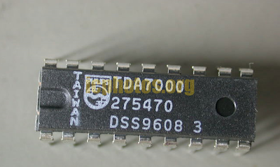
Here is a FM radio circuit using IC7400. IC TDA7000 is a monolithic integrated circuit for mono FM portable radios, where a minimum on peripheral components is crucial. The IC TDA7000 has a Frequency-Locked-Loop system with an intermediate frequency of 70 kHz. The intermediate frequency selectivity is achieved by active RC filters. The only function which needs alignment is the resonant circuit for the oscillator, thus selecting the reception frequency. Spurious reception is avoided by means of a mute circuit, which also eliminates too noisy input signals. Special steps are taken to meet the radiation requirements

Penerima Radio FmSkema Rangkaian Penerima Radio Fm


• L1 and L2 wind 5 turns of 0.6 mm enameled Copper wire on a 4 mm dia plastic former.


IC TDA7000 Description

The TDA7000 is a monolithic integrated circuit for mono FM portable radios, where a minimum on peripheral components is important (small dimensions and low costs).
The IC has an FLL (Frequency-Locked-Loop) system with an intermediate frequency of 70 kHz. The i.f. selectivity is obtained by active RC filters. The only function which needs alignment is the resonant circuit for the oscillator, thus selecting the reception frequency. Spurious reception is avoided by means of a mute circuit, which also eliminates too noisy input signals. Special precautions are taken to meet the radiation requirements.
IC TDA7000Lay out IC TDA7000


Data IC TDA7000

Supply voltage range: 2,7 to 10 V
Supply current : 8 mA
R.F. input frequency range: 1,5 to 110 MHz
Sensitivity for -3 dB limiting
• (e.m.f. voltage)
• (source impedance: 75 Ohm mute disabled) EMF: 1,5 uV
Signal handling (e.m.f. voltage)
• (source impedance: 75 Ohm) EMF typ. 200 mV
A.F. output voltage at RL = 22 kOhm75 Mv

Supply voltage: max. 12 V
Oscillator voltage: 0,5 to VP0,5 V
Storage temperature 55 to 150 C
Operating ambient temperature 0 to 60 C.

Pemancar FM dengan IC UPC1651

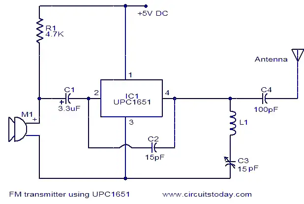
fm-transmitter-using-upc1651Here is the circuit diagram of an FM transmitter using the IC UPC1651. UPC1651 is a wide band UHF Silicon MMIC amplifier. The IC has a broad frequency response to 1200MHz and power gain up to 19dB.The IC can be operated from 5V DC.
The audio signals picked by the microphone are fed to the input pin (pin2) of the IC via capacitor C1. C1 acts as a noise filter. The modulated FM signal will be available at the output pin (pin4) of the IC. Inductor L1 and capacitor C3 forms the necessary LC circuit for creating the oscillations. Frequency of the transmitter can be varied by adjusting the capacitor C3.


Notes.

  • The circuit can be assembled on a Vero board.
  • Inductor L1 can be made by making 5 turns of 26SWG enameled copper wire on a 4mm diameter plastic former.
  • A ¾ meter insulated copper wire can be used as the antenna.
  • Do not give more than 6V to the IC.
  • Mic M1 can be a condenser microphone.

1 Watt Four Stage FM Transmitter

This FM transmitter circuit uses four radio frequency stages: a VHF oscillator built around transistor BF494 (T1), a preamplifier built around transistor BF200 (T2), a driver built around transistor 2N2219 (T3) and a power amplifier built around transistor 2N3866 (T4).

FM Transmitter circuit diagram

A condenser microphone is connected at the input of the oscillator. Working of the 1 Watt transmitter circuit is simple. When you speak near the microphone, frequency-modulated signals are obtained at the collector of oscillator transistor T1.

The FM signals are amplified by the VHF preamplifier and the pre-driver stage. You can also use transistor 2N5109 in place of 2N2219. The preamplifier is a tuned class-A RF amplifier and the driver is a class-C amplifier. Signals are finally fed to the class-C RF power amplifier, which delivers RF power to a 50-ohm horizontal dipole or ground plane antenna.
Use a heat-sink with transistor 2N3866 for heat dissipation (Note: or 2N4427 because it works better at 12 V and delivers up to 1 watt RF power). Carefully adjust trimmer VC1 connected across L1 to generate frequency within 88-108 MHz. Also adjust trimmers VC2 through VC7 to get maximum output at maximum range.
Regulator IC 78C09 provides stable 9V supply to the oscillator, so variation in the supply voltage will not affect the frequency generated. You can also use a 12V battery to power the circuit. Assemble the circuit on a general purpose PCB. Install the antenna properly for maximum range.
Coils L1 through L5 are made with 20 SWG copper-enamelled wire wound over air-cores having 8mm diameter. They have 4, 6, 6, 5 and 7 turns of wire, respectively.

3 Volt FM Transmitter

Rangkaian 3V FM Transmitter
Skema Rangkaian 3V FM Transmitter
This 3V FM transmitter is about the simplest and most basic transmitter to build and have a useful transmitting range. It is surprisingly powerful despite its small component count and 3V operating voltage. It will easily penetrate over three floors of an apartment building and go over 300 meters in the open air.

The circuit is basically a radio frequency (RF) oscillator that operates around 100 MHz. Audio picked up andamplified by the
electret microphone is fed into the audio amplifier stage built around the first transistor. Output from the collector is fed into the base of the second transistor where it modulates the resonant frequency of the tank circuit (the 5 turn coil and the trimcap) by varying the junction capacitance of the transistor. Junction capacitance is a function of the potential difference applied to the base of the transistor. The tank circuit is connected in a Colpitts

Place the transmitter about 10 feet from a FM radio. Set the radio to somewhere about 89 - 90 MHz. Walk back tothe FM transmitter and turn it on. Spread the winding of the coil apart by approximately 1mm from each other. No coilwinding should be touching another winding. Use a small screw driver to tune the trim cap. Remove the screwdriverfrom the trim screw after every adjustment so the LC circuit is not affected by stray capicitance. Or use a plasticscrewdriver. If you have difficulty finding the transmitting frequency then have a second person tune up and downthe FM dial after every adjustment. One full turn of the trim cap will cover its full range of capacitance from 6pF to 45pF. The normal FM band tunes in over about one tenth of the full range of the tuning cap.

So it is best to adjust it in steps of 5 to 10 degrees at each turn. So tuning takes a little patience but is not difficult. The reason that there must be at least 10 ft. separation between the radio and the FM transmitter is that the FM transmitter emits harmonics; it does not only emit on one frequency but on several different frequencies close to each other. You should have little difficulty in finding the Tx frequency when you follow this procedure.

Rangkaian Pemancar TV Sederhana

 Pemancar TV
Skema Rangkaian Pemancar TV Sederhana
This Transmitter Circuit TV uses standard 1 FM modulation for sound and PAL for video modulation. Audio signal will be modulated is pre-amplified using the transistor Q1 and associated components. The transistor Q2 has two jobs: production of carrier frequency and modulation. The pre-amplified audio signal is fed to the base of transistor Q2 for modulation. Capacitor C5 and inductor L1 forms the tank circuit which is responsible for producing the
carrier frequency. The video signal is fed to the emitter of transistor Q2 via POT R7 for modulation. The modulated composite signal (audio+video) is transmitted by the antenna A1.


Inductor L1 can be made by making 4 turns of 24SWG enameled copper wire on a 6mm dia: plastic former. T1 can be a radio frequency transformer with built in capacitor. (Can be found on old transistor radio boards). Antenna A1 can be a 1M long copper wire. (Experiment with the length to get optimum performance). This transmitter is working in VHF band somewhat between 50 – 210MHz. This transmitter is compatible only with PAL B and PAL G systems.

List Componet:
R1 = 10KOhm R2 = 47KOhm R3 = 15KOhm R4 = 8.2KOhm R5 = 47KOhmR6 = 47KOhm R7 = 1Kohm resistor variable R8 = 75Ohm C1 = 10uF/25Volt capacitor electrolik C2 = 0.001uf/10nF capacitor ceramic C3 = 100nF C4 = 10nf C5 = 47pF (variable capacitor) C6 = 10nF C7 = 10pF C8 = 27pF c9 = 100nF C10 = 470uF c11 = 10nF C12 = 220uF/25Volt Q1 = BC547 NPN transistor Q2 = BC547 NPN transistor
T1 = T1 can be a radio frequency transformer with built in capacitor. (Can be found on old transistor radio boards).
L1 = 4 turns of 24SWG enameled copper wire on a 6mm dia: plastic former.

FM Transmitter 12 Watt


The advantages of FM modulation is free from the influence of air disturbance, the bandwidth (wide band) is larger, and the high fidelitas. If compared with the AM system.

fm transmitter is a modification of the fm transmitter on the market (type of saturn s 038). with several series of modifications and additions boster series can produce power at around 12 watts


try in the series after this work is quite good, the signal generated is stable and strong enough
up time should not in a hurry to do directly, but overall do each part in sequence so that the error may be earlier

the first part of the work is in the oscillator, after the raft can try in turn to the way radio waves on the free and set the radio volume so clearly audible hissing sound. turn up the core koker hissing sound on the radio is missing, if you get a signal in a robust and stable means that the set of oscillator has been working with both.

the next section can start at the raft, after finished the second set trimer (C8 and C11) in the buffer in turn can power up in most large and most small SWR. If the series works well, will produce approximately 0.25 watt power

to get more resources than most can add more series boster 12 watt range, so the distance will be increased to reach 7-fold


12 watt Boster Circuit FM transmitter

FM Moulator with IC 555

FM Modulator circuit is a simple FM modulation circuit using IC 555, where the resulting modulated signal has a tenuous meeting depends on the signal frequency information. 

FM Moulator with IC 555

FM Moulator with IC 555 schematics

The resulting signal can be spelled out quite nice and stable so that the result will be more perfect. No winding or inductor in series modulator, so you do not need to bother to make a winding and calculate the value of the coil that you created it. With this circuit the desired value of frequency modulation can be obtained easily by calculating the frequency of IC 555 in general, which is determined by the resistor 6.8 K and 3.3 K and 0.1 UF capacitor. To obtain the other frequencies of your stay replace one or all three components.

Actually fm modulator ic 555 circuit is very simple though, but I think it reliable enough to handle a simple application purposes that do not require a big power or a very high frequency. But if you want more power you can add the RF amplifier circuit at the output of this circuit. Thus, the results of modulated signal can be amplified with the help of a series of supporters. In accordance with my experimental series modulators can work well at frequencies below the MHz range, because it is not IC IC 555 which is devoted to support of a very high frequency. You can use oscilltor transistor circuit, XTAL or others if you need a very high frequency.

The difference circuit with IC 555 on the multivibrator circuit in general is the use of pin 5, on the FM Modulator circuit is pin 5 of IC 555 is used as input information signal, which in turn will influence the shape of the output signal (modulated). But in applying this 5 pin multivibrator functions normally associated with 0.01 UF capacitor or left alone.

Transmitter - Received AM radio

AM Transmitter circuit 
To this powerful AM transmitters are huge, using ceramic tuning 3.587 mhz resonator and resonator filters are also sold with a value of 5.5 mhz, 7.7 mhz and 10.7 mhz. Distance transmitter range is approximately 2-4 km. the working principle of this circuit are filter resonator/ceramic filters raise the frequency of the value of the resonator filter.


This frequency is amplified by the transistor can be changed t1. Frequency so need C7 as a regulator / placement. sound signal superimposed over the audio transformer.frekuensi which awakened by resonator filters and t1 is fed to the next amplify strengthened so as to achieve the desired power passed to antenna. t2 and t3 as a buffer as a final power amp.


AM Transmitter Schematics


AM radio / receiver circuit
For AM radio because it's hard to find IC ZN 414 then now could be replaced with the equivalent of IC MK 484. Frequency coverage between 550 kHz-1600 mhz, 3 pins of this IC include series of radio tuner, RF amplifiers, automatic gain control, the AM detector. The series voltage regulator or a power transistor made by BC 108B, 4diada IN 4148, 2k7, 820R, and the 10K trimpot, trimpot functions for selectivity of the controller of all series. Then we using a booster class A and class B amplifier for signal modulated not disappear.

AM Received Schematics

TDA7012T - Single chip FM received

TDA7012T - Single chip FM received
FM Radio Receiver IC TDA 7012T is very simple, but Radio This FM receiver has good sensitivity and selectivity. Single Chip TDA 7012T FM Receifer is to build an FM receiver requires a few additional components.


Feature contained in FM receiver IC TDA 7012T is quite tempting to an FM receiver. Among features an FM receiver TDA 7012T is a low-voltage applications micro affability arrangement (MTS), Frequency Loked Loop (FLL) to 76 KHz range and selectivity of FM receiver with RC Filter. In an article by FM Radio Receiver IC TDA 7012T can be seen in the FM receiver circuit which can be made​​.

FM received Schematic
TDA7012T- Mini FM received Schematic
Part List
R1 = 8kΩ2
R2 = 10kΩ
R3 = 390Ω
C1,C3 = 10nF
C2,C6,C9,C16 = 100nF
C4 = 33pF
C5 = 25pF trimmer
C7,C10 = 1nF5
C8 = 820pF C11 = 1nF
C12 = 68pF
C13 = 220pF
C14 = 47μF 10V
C15 = 3nF3
L1 = 36nH
L2 = 1μH,
IC1 = TDA7021T

Radio remote controls for toy cars

Radio remote controls for toy cars (RC)
Playing cars that are controlled via radio signals is an interesting game. The much-loved toy cars children, plus a simple circuit will be the ideal toy car. This circuit families use traditional digital CMOS IC which requires very little electrical current, so it will not burden the original toy car performance.

In this system, radio signals are not transmitted continuously but only generated when the controller sends a command to the left / right or forward / backward, and even then only a radio-frequency discontinuous, so is sending pulses of radio wave frequency.

The number of pulses sent represent commands sent, GO command is represented with 8 pulses, is represented with 16 pulses LEFT, RIGHT DOWN 32 pulses and 64 pulses. Commands that can dikirimk is a combination of 2 orders once gus, which is a combination of command forward / backward and right / left, for example, could be sent forward orders and left once gus, in this case the number of pulses sent is 24, ie the sum of the forward command by 8 pulse and left the command of 16 pulses.

After a command is sent, the system stops sending commands in a certain time lag, the lag time it takes will be a series of recipients have sufficient time to fulfilling their orders well. Frequency pulses were visible on the right side of this.
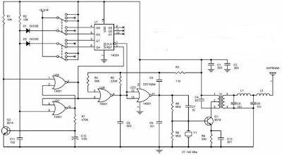


Radio Control Transmitter Series


How it works Transmitter
Radio signals generated by oscillator circuit formed by transistors Q1 9016, the working frequency of the oscillator is determined by the crystal Y1 is worth 27.145 MHz. A very critical part of this oscillator circuit is T1, L1 and L2, which specifically dealt with separately at the end of this article. Working from this oscillator is controlled by NOR gate U2D 14001, while the output gate (pin 3) is worth '1', the oscillator will work and transmit radio frequency 27.145 MHz, and at the output U2D value '0' the oscillator will stop working. U2D NOR gate receives the clock signal from NOR gate U2B. NOR Gate CMOS type with the aid of resistors R4 and R5 and capacitor C8 form a low frequency oscillator circuit for controlling the clock shaper of existing digital circuits. Work of this clock generator is controlled via the input leg 6, the circuit will generate the clock if this input berlevel '0 '.

NOR gate U2A and U2C form a series of Latch (RS Flip Flop), because of the influence of the resistor R2 and capacitor C11 is fed to pin 9 in U2C, when the circuit gets power supply output U2C must be '1 'and the output of U2A (leg number 3) becomes '0 '. This situation resulted Marja U2b clock generator works evoke reset the clock and remove the state of the enumerator 14 024 IC (U1), so that U1 started chopping and 27.145 MHz oscillator circuit sending pulses for generating a clock frequency of work.

At the start chopping, all the output of IC 14 024 enumerators in kedaan '0 ', after chopping 8 Q4 output pulse (pin 6) will be a '1', after counting 16 pulses output Q5 (pin 5) to '1 ', after chopping 32 Q6 output pulse (pin 4) to '1 ', after counting 64 pulses output Q7 (pin 3) to '1'.

Output over-output voltage used to control foot 9 U2C through diode D1 and D2, during one of the output is still worth '0 'then the clock generator U2B still working, this will continue until the cathode D1 D2 dankatode be '1' so that the foot 9 U2C be a '1 'as well. This situation will result in the output feet 3 U2A to '1 ', which stop the clock generator U2B and resets the enumerator 14 024 danberhenti already shipping 27 145 MHz pulse frequency.

To generate the lag time for receiver circuit has enough time carrying out orders, used a series of Q2 9014, resistor R7 and capacitor C10. The amount of delay time is determined by the value of R7 and C10. Switch to send command forward / backward and to send commands left / right are two separate switches. Each switch has 3 positions, the center position means that the scalar does not send commands.


Radio Control Receiver series

How it works Receiver
Figure 2 is a picture that matched the car receiver circuit toy, serves to receive signals from the transmitter to control motor cars, so cars can move forward / backward and left / right. Transistor Q1 with the help of resistors, capacitors and T1 form as a series of radio signal receiver 27.145 MHz. T1 in this series exactly the same as T1 that is used in the transmitter circuit, means of manufacture are discussed below.

Transistor Q2 follows perlangkapannya forming circuit to convert the radio frequency pulses received from the transmitter into the box pulses that can be accepted as a digital signal by the CMOS IC. Digital signal will be received as the clock had to be chopped by chopper 14 024 IC (U2). Output 14 024 will be in accordance with the number of pulses sent by the transmitter, forward command and left (which is used as an example in the discussion of the transmitter) is the pulse number of 24, the results of counting these pulses cause the output to be 14 024 Q4 = '1 ', Q5 = '1', Q6 = '0 'and Q7 = '0'.

Digital signal received in addition be used as a clock IC 14 024 enumerators U2 discussed above, used also to drive the 3 pieces of the time delay circuit to generate pulses which controls the circuit work.

Toll regulator will first appear after delivery frequency pulse stopped because the lag time between sending the code, this pulse serves to record the count results to the U3 14 024 14 042 (D Flip Flop), making the final conditions of 14 024 will be retained to control the motor. After the results were recorded to 14 024 14 042, 14 042 enumerator is reset by the second pulse, after the lag time for 14,042 enumerators can count start from 0 again.

The circuit formed by transistors Q3, Q4, Q7, Q8, Q9 and Q10 named as H Bridge circuit, this circuit is very reliable to drive DC motors. With this series of DC motor can be rotated to the right-to-left or stop motion. The main requirement of the use of this circuit is the base voltage of Q7 and Q10 base voltage must be opposed, for example base Q7 = '1 'and the base of Q10 = '0' the motor rotates to the left, the base of Q7 = '0 'and the base of Q10 = '1' the motor will spin to the right, the base Q7 = '0 'and the base Q10 = '0' motor stop motion, but it should not happen, the base Q7 = '1 'and the base of Q10 = '1'.

Similarly, Q5, Q6, Q11, Q12, Q13 and Q14 form a H Bridge. H Bridge to the left in Figure 2 is used to control motors that adjust the cars moving left / right, while the H Bridge right part is used to control motors that regulate movement forward / backward cars. The relationship between outpur enumerator 14 042 and 14 024 Input D Flip Flop is structured so that the signal is fed to each H Bridge can not be all '1 'simultaneously.

Making transformer TX and RX
Transformer T1 in series transmitter and receiver, is the same stuff, and have created their own. Transformer was built using plastic transformer Koker (spare part radio) that have a step that looks 5 lanes that can be filled with rolls of wire, as shown in the photo. Using this Koker facilitate wire transformer winding. If you can not Koker similar to it, just use the usual. Koker feritnya transformer is small and is also small (3 mm) as the first is often used for assembly of 27 MHz CB radio.

Wire to the transformer can wear a wire in the unloading of these Koker, carefully open coil of wire that already exist within the Koker because the wire is smooth and quite easy to break.

Step 1: Roll away from the feet of wire fed into the number 5 ft 4 in the direction h (CW) as much as 3 rolls right in level 1 (point level above the lowest point)

Step 2: Wind the wire from leg 1 to leg 2 in a clockwise direction as much as 4 rolls right on level 2.

Step 3: Continue the roll (from step 2) clockwise a quarter roll to as much as 3 feet 3 at level three. (Can be determined exactly a quarter of the roll, because kokernya have a path cut into 4).

Making coil L1
Wind the copper wire diameter of 0.3 to 0.5 mm by 10 quarter rolls on Koker diameter about 4 mm (which will be released), also in a clockwise direction.

Making coil L2
Wind the copper wire diameter of 0.1 mm by 50 rolls of plastic Koker without ferrite diameter of about 3.5 - 4 mm (look for plastic materials from used goods) are also in a clockwise direction. The length of the section in liputi rolls along the 5 mm.

USB FM transmitter circuit

USB to FM transmitter circuit


Here's a simple VHF FM transmitter that could be used to play audio files from an MP3 player or computer on a standard VHF FM radio. The circuit use no coils that have to be wound. This FM transmitter can be used to listen to your own music throughout your home. When this FM transmitter used in the car, there is no need for a separate input to the car stereo to play back the music files from your MP3 player.


To keep the circuit simple as well as compact, it was decided to use a chip made by Maxim Integrated Products, the MAX2606 [1]. This IC from the MAX2605-MAX2609 series has been specifically designed for low-noise RF applications with a fixed frequency. The VCO (Voltage Controlled Oscillator) in this IC uses a Colpitts oscillator circuit. The variable-capacitance (varicap) diode and feedback capacitors for the tuning have also been integrated on this chip, so that you only need an external inductor to fix the central oscillator frequency.
USB to fm transmitter schematics
USB FM transmitter schematics

It is possible to fine-tune the frequency by varying the voltage to the varicap. Not much is demanded of the inductor, a type with a relatively low Q factor (35 to 40) is sufficient according to Maxim. The supply voltage to the IC should be between 2.7 and 5.5 V, the current consumption is between 2 and 4 mA. With values like these it seemed a good idea to supply the circuit with power from a USB port.

A common-mode choke is connected in series with the USB connections in order to avoid interference between the circuit and the PC supply. There is not much else to the circuit. The stereo signal connected to K1 is combined via R1 and R2 and is then passed via volume control P1 to the Tune input of IC1, where it causes the carrier wave to be frequency modulated. Filter R6/C7 is used to restrict the bandwidth of the audio signal. The setting of the frequency (across the whole VHF FM broadcast band) is done with P2, which is connected to the 5 V supply voltage.

The PCB designed uses resistors and capacitors with 0805 SMD packaging. The size of the board is only 41.2 x 17.9 mm, which is practically dongle-sized. For the aerial an almost straight copper track has been placed at the edge of the board. In practice we achieved a range of about 6 metres (18 feet) with this. There is also room for a 5-way SIL header on the board. Here we find the inputs to the 3.5 mm jack plug, the input to P1 and the supply voltage. The latter permits the circuit to be powered independently from the mains supply, via for example three AA batteries or a Lithium button cell. Inductor L1 in the prototype is a type made by Murata that has a fairly high Q factor: minimum 60 at 100 MHz.

usb to fm transmitter pcb layout
Layout PCB USB FM transmitter

Take care when you solder filter choke L2, since the connections on both sides are very close together. The supply voltage is connected to this, so make sure that you don’t short out the USB supply! Use a resistance meter to check that there is no short between the two supply connectors before connecting the circuit to a USB port on a computer or to the batteries.

P1 has the opposite effect to what you would expect (clockwise reduces the volume), because this made the board layout much easier. The deviation and audio bandwidth varies with the setting of P1. The maximum sensitivity of the audio input is fairly large. With P1 set to its maximum level, a stereo input of 10 mVrms is sufficient for the sound on the radio to remain clear. This also depends on the setting of the VCO. With a higher tuning voltage the input signal may be almost twice as large (see VCO tuning curve in the data sheet). Above that level some audible distortion becomes apparent. If the attenuation can’t be easily set by P1, you can increase the values of R1 and R2 without any problems.

Measurements with an RF analyzer showed that the third harmonic had a strong presence in the transmitted spectrum (about 10 dB below the fundamental frequency). This should really have been much lower. With a low-impedance source connected to both inputs the bandwidth varies from 13.1 kHz (P1 at maximum) to 57 kHz (with the wiper of P1 set to 1/10).

In this circuit the pre-emphasis of the input is missing. Radios in Europe have a built-in de-emphasis network of 50 μs (75 μs in the US). The sound from the radio will therefore sound noticeably muffled. To correct this, and also to stop a stereo receiver from mistakenly reacting to a 19 kHz component in the audio signal, an enhancement circuit Is published elsewhere in this issue (Pre-emphasis for FM Transmitter, also with a PCB). Author: Mathieu Coustans, Elektor Magazine, 2009

MP3 FM Transmitter Parts List

Resistors (all SMD 0805)
R1,R2 = 22kΩ
R3 = 4kΩ7
R4,R5 = 1kΩ
R6 = 270Ω
P1 = 10kΩ preset, SMD (TS53YJ103MR10 Vishay Sfernice, Farnell # 1557933)
P2 = 100kΩ preset, SMD(TS53YJ104MR10 Vishay Sfernice, Farnell # 1557934)


Capacitors (all SMD 0805)
C1,C2,C5 = 4μF7 10V
C3,C8 = 100nF
C4,C7 = 2nF2
C6 = 470nF

Inductors
L1 = 390nF, SMD 1206 (LQH31HNR39K03L Murata, Farnell # 1515418)
L2 = 2200Ω @ 100MHz, SMD, common-mode choke, 1206 type(DLW31SN222SQ2L Murata, Farnell #1515599)

Semiconductors
IC1 = MAX2606EUT+, SMD SOT23-6 (Maxim Integrated Products)

Miscellaneous
K1 = 3.5mm stereo audio jack SMD (SJ1-3513-SMT
CUI Inc, DIGI-Key # CP1-3513SJCT-ND)
K2 = 5-pin header (only required in combination with 090305-I pre-emphasis circuit)
K3 = USB connector type A, SMD (2410 07 Lumberg, Farnell # 1308875)

Notice. The use of a VHF FM transmitter, even a low power device like the one described here, is subject to radio regulations and may not be legal in all countries.


source [ Link ]

RF-AF signal detector

RF-AF signal detector
The series that we will make this is a special electronic circuit can be used to detect the presence or absence of signal AF / RF. The circuit is very neat and simple to make. Costs it takes quite cheap. If you are already assembling this circuit, then with easy reader determine whether there is AF or RF signal at a particular section of a circuit.


Basic circuit uses an audio amplifier and a loudspeaker with switch input for AF and RF signals. The whole device can be made small as possible so it can be included in a container to maintain security. Audio amplifier section in this series created by IC TDA 2822M, with low stereo power amplifier in 8-pin mini-DIP. IC is used as a bridge cofiguration to shrink to 250 mW output power, loudspeaker handle 4 ohm, 500mW. The current required is less than 10mA with voltage of 3V battery.

schemaitcs signal RF-AF detector
RF-AF signal detector schematics


How it Works circuit


When the selector switch in the AF position, working on the input audio signal AF amplifier input (pin 7 of IC 1) through a capacitor C2 and potentiometer VR1. Capacitors C2 always hold input amplifier of the DC voltage and make it happen in the audio signal frequency. Input Signal IC 1 can be arranged with the help of potentiometers VR1.

When the selector switch in position RF and demodulator detector circuit formed by capacitor C1, diode D1, and resistors R1 and R2 are connected to the input The set. When the audio signal is detected then it will actually go kerangkaian to be strengthened. Signal detection is done by plugging probe (probe) on the legs of the existing components.

Simple FM transmitter with 2N3904

simple FM transmitter
In this section discuss about the series of mini fm transmitter, with broadcast coverage of about 300-400 meters. when using a 9 volt working voltage, the transmit power of about 300 meters and when using the working voltage 12 volts, the range of about 400-450 meters, depending on the antenna you use.

This scheme of simple fm transmitter
simple FM transmitter

For L1 and L2 windings 5 times the wrap, you can use a pen to fill melilitnya so neat and after lepaslah content of these pens. C5 is used for placement of broadcasting frequencies, can be tuned between 88-108 mhz, to reach further use steering antenna or Yagi antenna.

Part List
C1 = 0.001uF
C2 = 5.6pF
C3 = 10uF
C4 = 10uF
C5 = 3 - 18pF Adjustable capacitor
R1 = 270R
R2 = 4.7K
R3 = 10K
R4 = 100K
R5 = 4.7K
R6 = 4.7K
Q1 = 2N2222A
Q2 = 2N3904
L1 = 5 turn
L2 = 5 turn