Tampilkan postingan dengan label Microcontrol. Tampilkan semua postingan

Maybe we are more familiar with the term Minimum System AT89C2051 circuit, but this time I present a circuit which is not only a series of Minimum System AT89C2051 but more than that.

System circuit (not) Minimum (Evaluation Board) AT89C2051 and AT89C4051

The circuit is more deserves to be called Evaluation Board AT89C2051 and AT89C4051. Some of the advantages of circuit Minimum System AT89C2051 / AT89C2051 and AT89C4051 Evaluation Board which I was present this time, hardware-hardware support below:


RS-232 interface, DB-9
Header for LCD display
I2C, PCF8574 I / O extender
AT24C04, I2C EEPROM

DC motor driver with H-Bridge IC L293D

Making a DC motor driver with H-Bridge technique can use IC L293D as in the article "DC Motor Driver H-Bridge L293 (2 Motor DC)"is. DC motor driver L293D can be used to control the DC motor 2 pieces at once. DC Motor Driver L293D can be used to control a DC motor continuously or with a PWM technique. Dc motor driver circuit in the article "DC Motor Driver H-Bridge L293 (2 Motor DC)" only use IC L293D only. For more details see the following figure.


DC motor driver with H-Bridge  IC L293D

Working system of DC motor driver L293D is to provide control signals in the form of logic or pulse to the input lines 1A - 1B for DC motor control M1 and the input 2A - 2B for the control of DC motor M2 with the following conditions:
Input A Input B Motor DC
0 0 Motor silent
1 0 motor rotates counterclockwise
0 1 Motor berputer clockwise
1 1 Motor silent
Description: Enable Input given a logic 1 to obtain such data in the table above.

Read Only Memory

Memory group called Read Only Memory also has characteristics that match the name. Existing data in ROM, this is data that has been entered by the manufacturer. The data already contained in it can not be changed again through the normal process, and can only be read only. There are pieces of data in ROM is used for the identity of the computer itself. It is stored in the BIOS (Basic Input Output System). There are also data contained in this module was first accessed by a computer when it boots. Sequences contained in this module and are accessed the first time when the computer is turned on is called bootstrapping.


In this bootstrap process, carried out some instructions such as checking the internal components supporting the work of at least one computer system, such as checking ALU, CU, BUS supporter of the motherboard and processor, check the main BIOS, check the graphics card BIOS, check the Memory Module, check for the presence Secondary Storage which can be a floppy disk, hard disk, or CD-ROM drive, then just check the MBR (Master Boot Record) of the storage media designated by the BIOS (in the Boot Sequence). The following will be discussed types of ROM and its development.

PROM (Programmable ROM)
ROM provides an opportunity for users to modify data stored by default. A device called PROM programmer in charge of "burn" (burn in) this chip. With a strong electric current bit location will burn and showed a value (0 or 1). After going through the process burningin, this PROM can no longer be changed contents.

EPROM (Erasable Programmable ROM)
This chip is the development of PROM. Only, this EPROM can be erased its previous contents using ultraviolet light. These rays pass through a gap in the collection of chips. Thus, the charge stored can be released. In other words, EPROM can be erased with ultraviolet light and reprogrammed electrically.

EEPROM (Electrically Erasable Programmable ROM)
This chip is not much different from the EPROM, EEPROM data but can be removed without the use of ultraviolet light. Just use electrical pulses (electrical pulses). Types of ROM such as PROM, EPROM and 

EEPROM memory is classified into stable (nonvolatile memories). That is, these three types of ROM memory will keep its data even when not fed by electrical current. In development, the EEPROM chip has been used for the BIOS of a motherboard. By using the technique of "flash", the contents of the BIOS can be made later (update). However, the danger of flashable BIOS is all people can change the contents, including viruses. If you have been changed by a virus, then used a computer motherboard that will not be used again.

Universal PIC Programmer Circuit

Universal PIC Programmer Circuit
The series of Universal PIC Programmer can be used with software IC-Prog 1:05. Universal PIC programmer circuit is very simple with BC337 transistor 1 fruit, 2 pieces of IC regulators 7805 and 7808 as well as supporting passive components. Universal PIC Programmer series can be supplied with 2 pieces of 9V batteries.

For communication with computer circuit Universal PIC Programmer uses a serial RS232 port of computer. Then for the PIC to be programmed provided 5 lanes for the PIC that is DATA, Clock, Vpp, Vcc and Ground. For more details, can be directly seen in the figure below.

Universal PIC Programmer Circuit diaggram
Universal PIC programmer circuit diagram

The series of Universal PIC Programmer can be used to program the PIC family of 16F84A series, 12C509, 16C765 and the other. Hopefully this series of Universal PIC Programmer can help for friends who want to make PIC programmer.

Solid State Relay Circuit
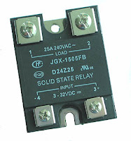
Solid state relay is a series that functions like a relay hibryd mechanics. Solid state relays is built with insulating an MOC for separate the input and the switch. With Solid state relays we can avoid the occurrence of sparks as it did in the relay can also avoid the occurrence of conventional connection is not perfect because porous contactor as in conventional relays.


The series of solid state relays This is quite simple and we can make in a PCB hole. For more details can be seen in the picture following a series of solid state relays.

Solid State Relay Circuit
Solid State Relay Circuit Diagram

Solid state relay has many advantages including no mechanical friction on the contactor, the connection process only occur when there are crosses zero, there is no spark at the contactor, not noisy, small konsusi flow control, better endurance.

DAC with MCS5 Microcontroller

DAC With MCS5 Microcontroller
The figure below shows the Configuration DAC With artificial MCS51 Microcontroller National Semiconductor, capacitors C1, C2 and form a series of 12 MHz XTAL oscillator, capacitor C3 and resistor R1 form a series reset.


Digital scale is given to the B1 to B7 (leg 5 to 12) in the IC DAC0800, the binary value of the digital scale was converted into an analog magnitude of the current at IOUT (ft 4 DAC0800) and IOUT * (feet 2 DAC0800), then by IC Operational Amplifier LM741 flow is converted into voltage. The resulting voltage expressed by the formula shown in Figure below, in addition to depending on a digital scale weight value is given, this voltage depends on the size of Vref (DAC0800 14 feet).

DAC With MCS5 Microcontroller
figure.1 DAC With MCS5 Microcontroller

C3 is mounted on leg 16 and ground is useful for stabilizing the voltage generated. DAC0800 and LM741 using voltage source +12 Volt and -12 Volt, is somewhat different from the voltage that is usually used for digital circuits, so that digital signals can be received well IC DAC0800, DAC0800 equipped foot VLC (pin 1) for various voltage levels menyesesuaikan types of digital ICs. In the DAC0800 data sheet are shown in various series to be installed on this leg for DAC0800 can be used for a variety of digital IC family. In the circuit of Figure above, the DAC0800 is connected to the microcontroller MCS51 family who work at TTL voltage levels, for this purpose VLC leg connected to ground.

Behind the legs of the IC DAC0800 B1 through B8 are not equipped to accommodate a latch that is fed a digital scale, changing the combination of digital signals on the legs is a direct result of output voltage change. Construction inputs such DAC0800, DAC0800 result can not be connected directly to a channel-data (data bus) microprocessor system, the relationship DAC0800 to the processor must pass through the parallel port.

In Figure 1, the DAC0800 is connected to the parallel port P1 from AT89Cx051. Connecting the DAC0800 to the other MCS51 family, for example AT89C51, can pass parelel ports P0, P1, P2 or P3, depending on the conditions established series. Instructions to remove the voltage in the circuit of Figure 1 is very simple, just use instruction MOV P1, A analog scale with the understanding that wish to be raised previously been stored in the accumulator A.

Making PC USB LCD controller project

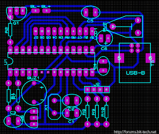
USB controller LCDThis really a work that so cool if you like modif PC. So this is a USB interface for alphanumeric LCD display like 4 × 20 which can be controlled with LCD Smartie program. USB interface is implemented by using PIC18F2550 microcontroller, Using USB LCD modules. Below is a project of the USB LCD controller.


Schematic circuit and PCB design
Schematic USB control LCD

USB to control LCD from PC

source  | link